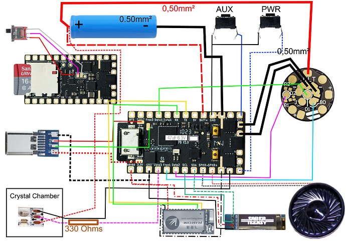
It might be easier to see once the circuit diagrams are up (which I will put up this weekend), but it’s really quite straightforward, and what is connected to what is spelled out in the “pin function table” on the V3 page:
https://fredrik.hubbe.net/lightsaber/v6/
Let’s take the “Free 3” pad as an example.
It’s hooked up to two pads on the CPU: PB11 and PC2.
PB11 has several functions: GPIO, PWM/Servo and TX4
PC2 also has several functions: GPIO, Analog and MISO2
(TX4 just means TX pin for the fourth serial port bw.)
SInce they are hooked up together, the “Free 3” pad can do all of these things.
However, it cannot do two things at the same time. The simplest example would
be if we try to do something like:
digitalWrite(9 /* PB11 */, HIGH);
digitalWrite(10 /* PC2 */, LOW);
This will create a short, and power will flow directly from one pin to the other, which can potentially damage something.
Using one pad as an input, and the other as an output would be harmless though, like:
digitalWrite(9, HIGH);
analogRead(10);
For the most part, the V3 pin map only lists one of the two pins when they are linked, which means that as long as you’re using symbolic names, it’s very difficult to mess up and damage something.
I also plan to add some code to ProffieOS which will keep track of these linked pins and prevent you from trying to use them for two things. For now there are no protections, but we also don’t use most of the functions, so it’s not very easy to do something that would be bad.
