I was looking at the schematic for the Proffieboard V3.9 and had a question about Q7B (reverse polarity protection FET).
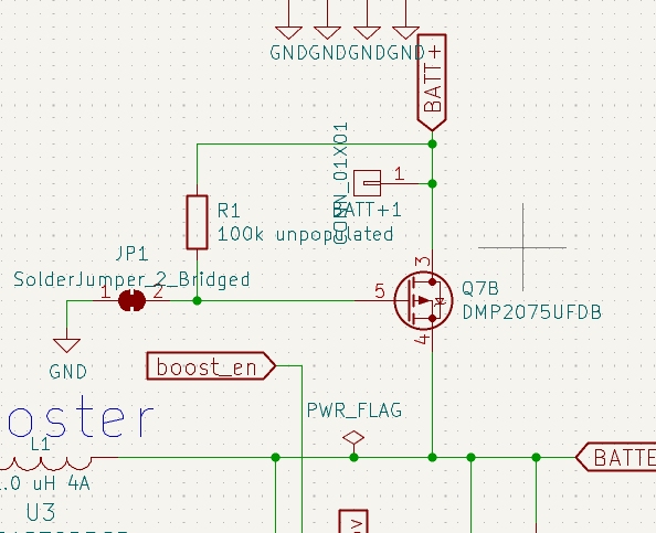
If I am reading the schematic right, the body diode of the FET conducts all of the current for the board when the battery is connected correctly. However, I don’t see how the gate gets biased to turn the FET on. Shouldn’t R1 should be between GND and the gate?
Without the solder jumper bridged, the Gate is pulled up to Batt+ and the FET never turns on…unless I am missing something?