jlc PCBs? I wonder if they can do it. they say their bga can do .25 pad size with .12 in-between on their 4/6 layer pcbs. which the .4 pads and .18 inspace falls into. I am using easyeda so its easy to order from.
That just means that they can make the grid of pads.
They don’t have any way of “escaping” the grid. (making traces from inside the grid, to outside the grid.) AFAIK, there is no way to escape a 7x7 grid with 0.4mm separation without stacked microvia capabilities.
You right jlc doesnt support blind vias but pcb way does. Which I have heard its hit or miss with them.
Regular blind vias is also unlikely to work.
The vias would have to be very small (like 0.3mm) which I don’t know of any manufacturer that supports. And even if they were that small, you would need a custom stackup, as you would need at least three different depths of vias to make it work.
micro-vias are laser-drilled, and has no insert, so they can be much smaller than regular vias. This sort of PCB construction is called HDI, and seems to be expensive enough to be difficult for hobbyists to get in to unfortunately. Because the vias are so much smaller, it should be possible to place them off-center in the pads, making space for traces in between them which I think means you only need two different depths of vias.
Also, laser-drilled micro-vias apparently require no “annular ring”, which helps a lot with density.
yep, the HDI is super expensive there goes the Idea for the BGA stm32l433cc.
The 8x8 BGA with 0.5mm separation might be manageable on the new oshpark 6-layer service,
especially since we won’t need to get traces to all the pins. It might require a trick which only some PCB design programs can do though: Vias with with no annular ring on unconnected internal layers. Last I checked, it was difficult to get kicad to do this, but not impossible. I’m not sure if kicad V6 is any better at it. With no annular ring, there should be enough space between vias to fit a trace between them I think. (on internal layers)
Well I will try and see if I can get kicad up and running. and then see how small I can make the board as is if I lose the booster and some of the fets. Any suggestions on subs for the fets. as the current ones are not in stock and maybe I can save some space.
There is a whole bunch of compatible ones with the same footprint. As for smaller ones, I have not looked.
as my goal for this one is a blaster. it will be running 20 to 30 neopixels. so such a high amp rating is unnecessary, I will take a look around
Since my goal would be to make something that is useful to as many people as possible, using high-amp FETs is a requirement for me.
I will use the same footprint. I found some different rated ones that were available. Besides all the most obvious pads. what do you think should be removed, pad wise? I am thinking about losing these pads. and losing mosfets 4-6 and maybe 3 as well. And one of the resistor bars.
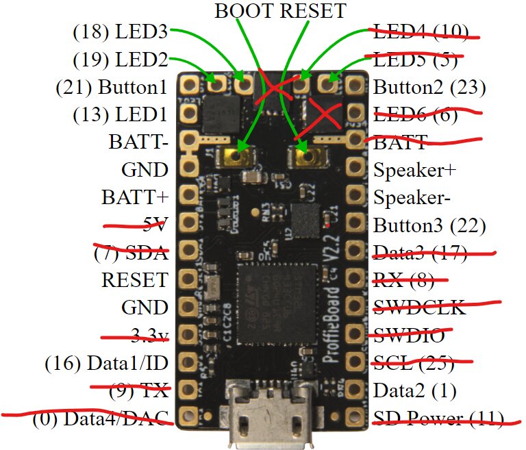
Is there any really good reason to keep any of these that I marked off?
1 Like
RX/TX: fine if you don’t need bluetooth
SDA/SCL: fine if you don’t need displayss
SWDIO/SWDCLK: are helpful for test rigs
For your own purposes you probably don’t need any of those though.
Ooh let me know when you’ve made a test run, and I’ll buy one off you for testing and feedback.
Most likely it will take a while.
I can’t find the chips for sale anywhere.
Same, if you make a v2.2 or 3.0 mini. I will totally test and do a mini built in a saber give feed back. I am very flexible and have a solid basic understanding of electronics. Ok its probably intermediate level. I feel like I am still learning.
Hopefully I will be able to do my proffie-T build soon. T is for tactical or Tano or tiny. I am starting to see parts pop up so maybe its starting to get back to normal. BTW is there anyway to change my user name from gammax to Lady Tano?
fun fact GammaX is for my two favorite types of ionizing radiation.
Time for a teaser pic:
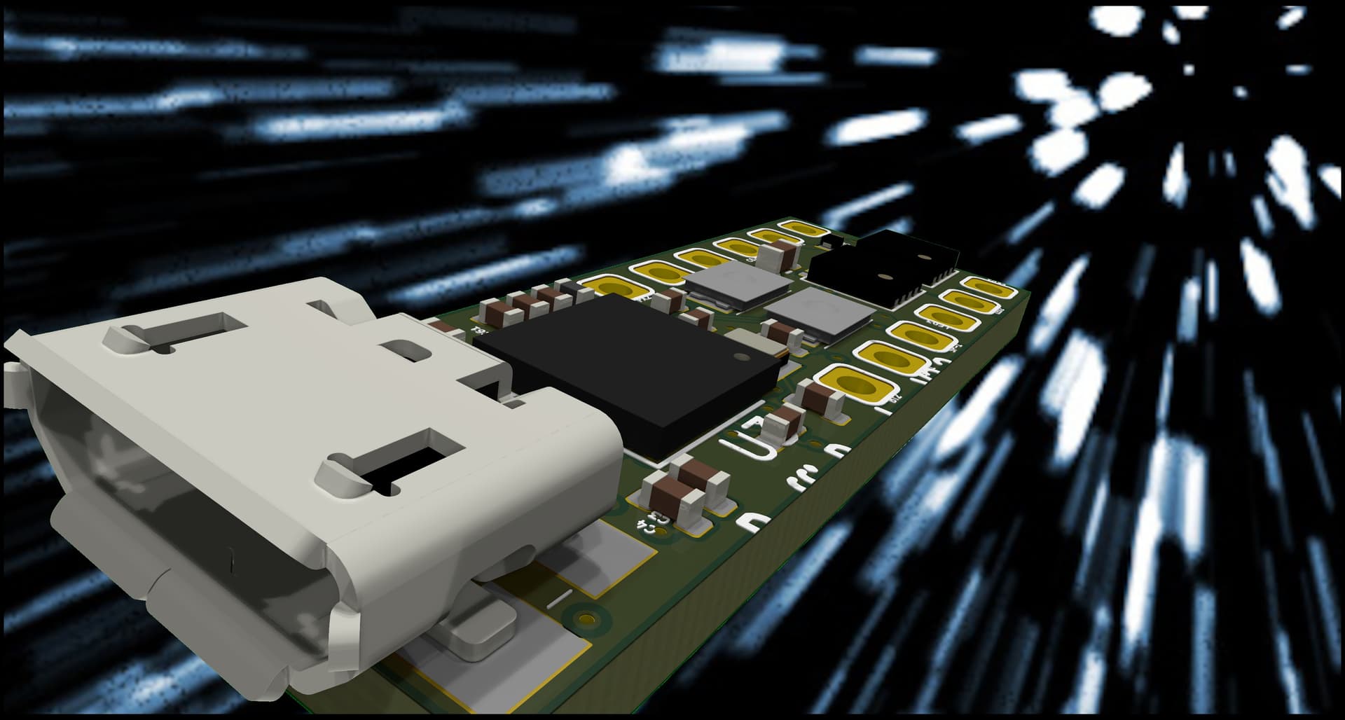
This thing is 10x28mm (plus 1-2mm because of the usb port sticking out.)
I managed to route it, but there is a lot of cleanup to do.
Also, I can’t make it because I can’t find the chips for it. 
3 Likes
So sleek and streamlined. You should call it the proffie slim. =P
Looks awesome to me. it will put be together when parts are available again. That’s going to be great with a sonic… Btw did you include the booster or is it left out of this one? if you left it out, It looks like I can maybe add it to a connector board. As I might need it if I make a strip of the 1515 w2812b. It might have like 40 or more, depending on how many I can stuff on the barrel.
You arent updating it to usb c?
USB-C is bigger.
I might upgrade to USB-C eventually, but I’m not in any hurry, and it doesn’t seem right for this board, which for the record shall be called “Proffieboard M2”, (M for Mini, 2 because it’s basically a Proffieboard V2)
It does not have a booster. Not sure why you would need a booster to drive WS2812b LEDs, they are quite happy with battery voltage. The booster on the V2 boards are only used to make the sound louder.
Oh I didnt know thats what its main purpose is for boosting the sound. Make sense. I thought it was fro driving the leds. Since there are about 200+ LEDs usually in most sabers. I figure 5v is what the w2812s are most happy at. But KISS for sure.
Because of the voltage drop that occurs in long lines of neopixels, ws281x chips have to accept a fairly wide range of input voltage. One of the tricks they use is a constant-current LED driver. This constant-current LED driver means that once the voltage is high enough, increasing it any more does not make the LEDs brighter, it just makes the control chip hotter. What “enough voltage” is is somewhere around 3.5 volts in most neopixels. Below that, the green color stars to fade, and then the blue color. Once you get down to ~2 volts, only red remains.