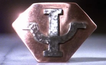
I think I have a strong naming candidate:
Proffieboard SI, Or PSI, or Ψ.
PSI and ESP both alludes to extra-sensory-perception, which sort of makes sense for things that are wireless. Also:

I think I have a strong naming candidate:
Proffieboard SI, Or PSI, or Ψ.
PSI and ESP both alludes to extra-sensory-perception, which sort of makes sense for things that are wireless. Also:

lol, I like it.
Edit: My background is in physics, so I am always happy to see psi pop up when it can. ![]()
Did some pin counting.
It looks like the ESP32-S3 chip itself is the only one that has enough GPIOs, so I guess I won’t be using any of their ready-made modules. It’s their latest and greatest chip, so it’s the chip I want to use anyways.
update:
That turns out to be a misread of the data sheets. On the ESP32-S3-MINI-1 module, there are six pins that are not connected to anything, which I thought meant that the chip had more GPIOs than the module - wrong. These pins are connected to the flash chip inside the module itself, and cannot be used for anything else. That makes the GPIO count fairly tight, but it might still work. The modules and the chip itself have the same number of GPIOs available though.
Question for the sake of curiosity: I was poking around on mouser, and found the microcontroller section (All Products Semiconductors Integrated Circuits - ICs Embedded Processors & Controllers Microcontrollers - MCU). In that section there are lots of devices with more than 45 io pins, and that got me wondering. What is the difference between devices in this section and the devices (like esp32) that we use on the proffieboard? Are the microcontroller devices completely different kinds of devices?
There is no difference, but 35+ pins is far from the only requirement for a good Proffieboard microcontroller though, here is a partial list:
Porting proffieOS to a new CPU is a bit of work, which makes this a “pick one and focus on it” process rather than a “try to support everything” process.
It’s growing on me… Ok, I like it. I approve ![]()
I honestly read the entire thread (I’m old), and I don’t see NFC mentioned as an option for wireless transfer. Perhaps the inductive coupling is downright impossible through metal? And the antenna is bulky. And the hardware is not included on most CPU boards. Actually, never mind…
NFC is super slow.
It could be a way to initiate a connection though. Of course, it requires hardware both in and out of the saber, which makes it a bit cumbersome.
That said. I have a feeling that I’m going to have to keep the USB connector.
ESP32-S3 has support for debugging over USB, and if that works well, then I can use four pads on the CPU for something else, which I think I need in order to make the whole thing work.
Fitting everything on the board is going to be pretty tight, but that’s also the fun part. ![]()
Ideas for saving space on the board:
I would think that single sided pads across the board could effectively double the real estate. No NEED to have thru holes, right?
I imagine some folks would prefer through holes…… for some reason. I’m in the smt camp though.
In theory yes, but pads that only exists on the top of the board are hard to test. It would require some sort of setup which has pogo pins both on the top and on the bottom…
On the M2 board I put some pads on the bottom, and used the top for components.
Through-hole is much easier to solder since you can secure the wire to the hole before applying solder, and the resulting solder joint is much stronger too. However, easier isn’t always better…
ah, I hadn’t thought of it being stronger… as for easier, yeah, but personally I think through-hole joints are ugly as sin because of the stabby bit that sticks up or down, so my aesthetic preference is to just solder to the surface. But I hadn’t considered strength, which could have significant benefits for this application, what with the whackin and the bangin. I imagine there may be significant fatigue effects… which leads me to wonder if any particular blend of solder is better than others for resisting fatigue fracture? I know non-eutectic formulas tend to get the frosty crystallized surface effect, but I don’t recall off the top of my head what the crystallization behavior is under the surface… might have to buzz my old manufacturing professor who specializes in metal casting. or google. google might work too. ![]()
I don’t have a good answer for this, but it seems like harder/stronger solder requires higher temperatures, which is not a great trade-off when working with electronics.
well, in this case I don’t think we want HARDER solder, as metals (and pretty much everything) become more prone to brittle fracture as hardness increases. Hardness is usually due to the microcrystalline structure in the material. If you can keep it amorphous, that tends towards softness, and thus less brittle. all materials are different of course, and I don’t remember the characteristics of solders. Fortunately for us, lead is a super ductile material to begin with, and there’s lots of stuff you can alloy it with to change the properties. I’m sure many phd thesis have been done on the topic. Just need to figure out how to find those results.
That is the most brilliant innovation in my book. This would simplify soldering, cable routing and probably board layout.
The antenna is definitely going to be the hardest part about building an ESP32-based proffieboard, and regardless of how well the antenna is designed, once we shove it in a metal hilt full of cables and plastic, who knows if it will even work? Proper antenna design requires that you know what the antenna is made of, how wide/long/thick it is and what it is surrounded by. Especially that last part is going to be a big “no idea” in a saber sound board.
Let me lay out the options I’m aware of:
Some spitball ideas coming from a background of limited electronics knowledge:
Can a pcb trace antenna be embedded in an internal layer of the board? could be used as a backup or fall back option if you wanted to use an external antenna connector as the primary antenna.
Can a chip antenna be put on a tiny separate pcb, which would then be wired to the main pcb? I’m thinking about the bourns battery connectors that I’m using in the bayonet lug connector. I have the male connectors in the main chassis, and then a small pcb that stays with the aluminum body and allows the signals (originally intended to just be buttons) to be routed through the 16mm button hole. I’ve got 10 poles in the current design, so there are way more than are needed for a simple button. Some of them could be repurposed to provide a connetion between PB and a chip antenna that is located on a tiny pcb on the exterior of the saber (presumably covered by plastic.
This antenna chip might be interesting though:
It is designed to sit directly over a ground plane. That should mean that I can still use the other side of the board for pads or components.
Interesting. So time for a story: waaay back in the olden days, I was a high frequency radio operator in the us army. Amongst the many pieces of antique equipment we were trained on was a particular device whose purpose it was to ensure that the signal from the radio could be transmitted from an antenna of fixed length, regardless of frequency. Normally, your antenna has to be a multiple or fraction of the wavelength of the frequency you’re trying to transmit on, and if it’s not then the signal will ‘bounce back’ and be severely attenuated. So the device, whose name escapes me, helps prevent that bounce back. I forget how it all works, unfortunately. Anyway, my point is that if such a device could be made in a small enough package one could hypothetically be surface mounted on an external antenna trace or chip holding pcb. Totally BSing my way through this, but you get the point. Maybe even have an external radio smd component that talks to the pb over i2c or something.
I’m not sure if you’re referring to impedance matching, which is required for good antenna operation. Adaptive antennas (for different frequencies) is an area of active research where people are experimenting with all sorts of weird stuff, but fortunately we don’t need that since all the traffic will be at ~2.45Ghz